ASIC design is all about juggling multiple competing requirements. You want to make the chip competitive by increasing its capabilities, by reducing its price, or both. Today we'll focus on the second half of that tradeoff, reducing the price.
Chip fabrication is a statistical game: of the parts coming off the fab, some percentage simply do not work. The vendor runs test vectors against the chips, and throws away the ones which fail. This is called the yield, and is the primary factor determining the cost of the chip. If the yield is bad, so you have to fab a whole bunch of chips to get one that actually works, you have to charge more for that one working chip.
To illustrate why most chips coming out of the fab do not work, I'd like to walk through part of manufacturing a chip. This information is from 1995 or so, when I was last seriously involved in a chip design, and describes a 0.8 micron process. So it is completely old and busted, but is sufficient for our purposes here.
Begin by placing the silicon wafer in a nitrogen atmosphere. You deposit a photo-resist on the wafer, basically a goo which hardens when exposed to ultraviolet light. You place a shadow mask in front of a light source; the regions exposed to light will harden while those under the shadow mask remain soft. You then chemically etch off the soft regions of the photo-resist, leaving exposed silicon where they were. The hardened regions of photo-resist stay put.
Next you heat the wafer to 400 degrees and pipe phosphorous into the nitrogen atmosphere. As the K atoms heat they begin moving faster and bouncing off the walls of the chamber. Some of them move fast enough that when they strike the surface of the wafer they break the Si crystal lattice and embed themselves in the silicon. If they strike the hardened photo-resist, they embed themselves in the resist; very, very few are moving fast enough to crash all the way through the photoresist into the silicon underneath.

Next you use a different chemical process to strip off the hardened photoresist. You are left with a wafer which has phosphorous embedded in the places you wanted. Now you heat the wafer even higher, hot enough that the silicon atoms can move around more freely; they move back into position and reform the crystal lattice, burying the phosphorous atoms embedded within. This is called annealing. Now you have the p+ regions of the transistors.
You repeat this process with aluminum ions to get the n- regions. Now you have transistors. Next you connect the transistors together with traces of aluminum (which I won't go into here). You cut the wafer to separate the die, and place each die in a package. You connect bonding wires from the edge of the die to the pins of the chip. And voila, you're done.
It should be apparent that this is a probabalistic process. Sometimes, based purely on random chance, not enough phosphorous atoms embed themselves into the silicon and your transistors don't turn on. Sometimes too much phosphorous embeds and your transistors won't turn off. Sometimes the Si lattice is too badly damaged and the annealing is ineffective. Sometimes the metal doesn't line up with the vias. Sometimes a dust particle lands on the chip and you deposit metal on top of the dust mote. Sometimes the bonding doesn't line up with the pads. Etc etc.
This is why the larger a chip grows, the more expensive it becomes. Its not because raw silicon wafers are particularly costly, its that the probability of there being a defect somewhere grows ever greater as the die becomes larger. The bigger the chip, the lower the yield of functional parts.
 For at least 15 years that I know of, chip designs have improved their yield using redundancy. The earliest such efforts were done in on-chip memory: if your chip is supposed to include N banks of SRAM, put N+1 banks on the die connected with wires in the top most layer which can be cut using a laser. The SRAM occupies a large percentage of the total chip area, statistically it is likely that defects will be within the SRAM. You can then cut out the defective bank, and turn a defective chip into one that can be used. More recent silicon processes use fuses blown by the test fixture instead of lasers.
Massively Multicore Processors
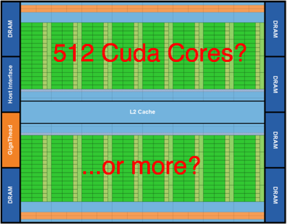
Yesterday NVidia announced Fermi, a beast of a chip with 512 Cuda GPU cores. They are arranged in 16 blocks of 32 cores each. At this kind of scale, I suspect it makes sense to include extra cores in the design to improve the yield. For example, perhaps each block actually has 33 cores in the silicon so that a defective core can be tolerated.
In order to avoid having weird performance variations in the product, the extra resources are generally inaccessible if not used for yield improvement. That is even though the chip might have 528 cores physically present, no more than 512 could ever be used.
