Showing posts with label embedded. Show all posts

Thursday, March 27, 2025

Macbook Air M1 USB-C Port Replacement

My Macbook Air M1 was gradually developing some kind of impairment in its USB-C ports where I'd have to jiggle or put actual pressure on a USB-C cable to get it to be recognized — and since it has no Magsafe port for charging, this meant it would switch to and from battery as its charging cable periodically lost contact.

Searching turned up people reporting similar issues, especially that the rear port started having a problem first until eventually the front port did as well. There wasn't a consensus solution but a replacement USB-C board from iFixit came up several times. For only $20, I ordered one.

Innards of a Macbook Air M1, with the old USB-C board off to the side and the new board installed

The original USB-C board is off to the right side in this picture. One can see some corrosion and dirt, and also a bit of blackening on what I assume is a power pin. I believe that carbon buildup is likely the primary issue. I'll scrub it off with some alcohol on a cloth and put it away for the future, it would probably work again if needed.

Saturday, September 15, 2018

The Arduino before the Arduino: Parallax Basic Stamp

I recently had cause to dig down through the layers of strata which have accumulated in my electronics bin. In one of the lower layers I found this bit of forgotten kit: the Parallax Basic Stamp II. This was the Arduino before there was an Arduino, a tiny microprocessor aimed at being simple for hobbyist and low-volume commercial use.

The Basic Stamp line is still sold today, though with designs developed over a decade ago. The devices have enough of a market to remain in production, but are otherwise moribund. The past tense will be used in this blog post.

The Basic Stamp line dates back to the early 1990s. The Basic Stamp II shown here was introduced in 1995. It used a PIC microcontroller, an 8 bit microprocessor line which has been used in deeply embedded applications for decades and is still developed today. The PIC family is a product from Microchip Technology, the same company which now supplies the AVR chips used in the Arduino after acquiring Atmel in 2016.

The PIC contained several KBytes of flash, which held a BASIC interpreter called PBASIC. An external EEPROM on the BS2 board contained the bytecode compiled user BASIC code. Though it may seem an odd choice now, in the early 1990s the choice of BASIC made sense: the modern Internet and the Tech industry did not exist, with the concordant increase in the number of people comfortable with developing software. BASIC could leverage familiarity with Microsoft GW-BASIC and QBASIC on the PC, as MS-DOS and Windows computers of this time period all shipped with BASIC. Additionally, Parallax could tap into the experience of the hobbyist community from the Apple II and Atari/Commodore/etc.


' PBASIC code for the Basic Stamp
LED         PIN 5
Button      PIN 6    ' the BS2 had 16 pins
ButtonVal   VAR Bit  ' space is precious, 1 *bit* storage
LedDuration CON 500  ' a constant

' Init code
OUTPUT LED
INPUT  Button

DO
 ButtonVal = Button                 ' Read button input pin
 FREQOUT LED,LedDuration,ButtonVal  ' PWM output to flicker LED
 PAUSE 200                          ' in milliseconds
LOOP

PBASIC supported a single thread of operation, the BASIC Stamp supported neither interrupts nor threads. Applications needing these functions would generally use a PIC chip without the BASIC interpreter on top. Later Stamp versions added a limited ability to poll pins in between each BASIC statement and take action. This seemed aimed at industrial control users of the stamps, for example Disney used BASIC Stamps in several theme park rides designed during this time frame.

A key piece of the Arduino and Raspberry Pi ecosystems is the variety of expansion kits, or "shields," which connect to the microprocessor to add capabilities and interface with the external world. The ecosystem of the BASIC Stamp was much more limited, suppliers like Adafruit were not in evidence because the low volume PCB design and contract manufacturing industry mostly didn't exist. Parallax produced some interesting kits of its own like an early autonomous wheeled robot. For the most part though, hobbyists of this era had to be comfortable with wire-wrapping.

Friday, September 15, 2017

On CPE Cost

When it comes to the cost of hardware, volume matters more than anything else. To large extent, volume matters more than everything else put together. A cost efficient hardware design produced in low volume will be considerably more expensive than an inefficient and sloppy design produced in high volume. Plus, for a high volume product, the Contract Manufacturer will have engineering teams to help tighten the design for a moderate fee.

If your own sales volume is sufficient to get deep volume discounting, you can stop reading now (more honestly, you aren't reading this in the first place). Otherwise, if you are building a product for a new market or you are building for a niche, read on.

What does this mean? It means you should work very, very hard to use hardware which is produced in high volume. The compromises you would make in terms of RAM or other capabilities in order to get your own custom design down to a price you can tolerate will cost you far more than you saved in terms of updating the software and capabilities throughout the service lifetime. Using an existing, high volume design may bring other compromises, but it is a good tradeoff to make.

If you want to have your branding on the box: many commercial off the shelf (COTS) devices are available in unbranded white-box versions. It is simple and easy to add silkscreening or design flourishes, often a one-time design fee and a tiny line item on the Bill of Materials.

If you want to add RAM, Flash, moderately faster CPU, etc: most of those white-box products allow customization of specs which do not require changes in the board design. RAM and Flash suppliers offer different capacities in the same pinout, and CPU vendors offer multiple speed-bins of their chips. There will be a sweet spot in the market where the industry is buying the most volume, with a reasonable standard deviation such that you can moderately increase the capability without substantially increasing the cost. The converse is also true: moderate reductions in RAM/Flash/CPU don’t substantially decrease cost and may not be a good tradeoff.

If you want to have a unique industrial design: many ODMs will customize a product for you, including a new casing. It will need to fit the existing board, and will cost a few hundred thousand dollars for design, tooling, and emissions testing, but that is still cheaper than taking it all on in-house as you get the volume pricing for the board and other components.

Corollaries:

  • Mobile ate the world. You shouldn’t shy away from using mobile chipsets, even if your product will never operate on battery. Volume drives cost down, and mobile has the volume. Also, mobile chipsets with good power management are less in need of active cooling, and fanless is a huge win for consumer products.
  • RAM does cost money, but RAM is your future proofing. Greatly reducing RAM to lower cost is usually a bad tradeoff. Raspberry Pi Zero has 512 MBytes of RAM and costs US $10. Moderate amounts of RAM do not add much cost.
  • Many modern CPUs have configurable endianness, but seriously: little endian won. I hate that it won, but it did. If you’re considering a big endian toolchain, think carefully about the life choices that led you to that dark place. You’ll be taking endianness bugs onto your own plate for no benefit.

Monday, September 11, 2017

Musings On Customer Premises Equipment

I spent most of the period 2011 - 2017 building Customer Premises Equipment (CPE) for an Internet and television service provider. CPE gear is equipment which is installed in a customer’s residence/business/etc in order to provide an endpoint for whatever service the provider offers. For an Internet Service Provider this will be things like cable/DSL modems and Wi-Fi routers. For an electric utility, the remotely accessible meter could be considered the CPE. There are very few services which don’t require any sort of equipment on premises.

CPE devices are built very much like other consumer electronics, using the same components and software techniques. The biggest distinction is in the mindset for its development: the device you are building is not the product. The device you are building is an enabler, the actual product is the service being offered. It might seem a minor distinction but, done right, it shouldn’t be minor. It should influence the entire implementation.

For example, comparing consumer electronics built for sale to end-users to CPE devices used by service providers:

  • Devices for retail will build several variants, leveraging the same development and codebase but providing multiple price points for different market segments. They may also have slightly differentiated SKUs for large retailers to not compete directly with each other on price. For a service provider CPE, the incentive is the opposite: just one model to avoid inventory cost and CPE replacement for customers who upgrade. Multiple price points are provided by the service plan, which means the CPE will have capabilities which are not enabled for customers on the lower tier plans.
  • Devices sold to end-users will often cater to power users, as getting good reviews and positive press leads to increased sales in the vastly larger mid-tier market. They will have long lists of features, and try to check as many boxes as possible. For a service provider CPE, obscure features add support costs without attracting much additional market share. The CPE will usually target the 80% point of features which will be widely used. The kind of customer who really wants the power-user features tends to also be the most likely to try to Bring Their Own Device and make minimal use of the provided CPE, anyway.
  • For a CPE device, remote serviceability is a hugely important feature. Ability to resolve a customer escalation without having to send a technician is important for OpEx (Operational Expense). Even if the service provider charges for technician visits, it is at best defraying costs and not enough to incentivize wanting to send techs.
  • Though upfront capital cost is important, the service lifetime of CPE in the field is equally important. The value of CPE devices is in the ongoing service revenue they enable. It makes sense to leave headroom in the initial device to be able to support upgraded services in the future, and is financially preferable to having to retire the device earlier. Retirement either means mass replacement of customer devices, or writing off a portion of the customer base for any future offerings and just leaving them as is.

I found the work on CPE devices to be interesting. I hope to write about a few areas of it.

Thursday, February 9, 2012

ATA Commands in Python

In software development sometimes you spend time on an implementation which you are unreasonably proud of, but ultimately decide not to use in the product. This is one such story.

I needed to retrieve information from an attached disk, such as its model and serial number. There are commands which can do this, like hdparm, sdparm, and smartctl, but initially I tried to avoid building in a dependency on any such tools by interrogating it from the hard drive directly. In pure Python.

Snicker all you want, it did work. My first implementation used an older Linux API to retrieve this information, the HDIO_GET_IDENTITY ioctl. This ioctl maps more or less directly to an ATA IDENTIFY or SCSI INQUIRY from the drive. The implementation uses the Python struct module to define the data structure sent along with the ioctl.

def GetDriveId(dev):
  """Return information from interrogating the drive.

  This routine issues a HDIO_GET_IDENTITY ioctl to a block device,
  which only root can do.

  Args:
    dev: name of the device, such as 'sda' or '/dev/sda'

  Returns:
    (serial_number, fw_version, model) as strings
  """
  # from /usr/include/linux/hdreg.h, struct hd_driveid
  # 10H = misc stuff, mostly deprecated
  # 20s = serial_no
  # 3H  = misc stuff
  # 8s  = fw_rev
  # 40s = model
  # ... plus a bunch more stuff we don't care about.
  struct_hd_driveid = '@ 10H 20s 3H 8s 40s'
  HDIO_GET_IDENTITY = 0x030d
  if dev[0] != '/':
    dev = '/dev/' + dev
  with open(dev, 'r') as fd:
    buf = fcntl.ioctl(fd, HDIO_GET_IDENTITY, ' ' * 512)
    fields = struct.unpack_from(struct_hd_driveid, buf)
    serial_no = fields[10].strip()
    fw_rev = fields[14].strip()
    model = fields[15].strip()
    return (serial_no, fw_rev, model)

No no wait, stop snickering, it does work! It has to run as root, which is one reason why I eventually abandoned this approach.

$ sudo python hdio.py
('5RY0N6BD', '3.ADA', 'ST3250310AS')

HDIO_GET_IDENTITY is deprecated in Linux 2.6, and logs a message saying that sg_io should be used instead. sg_io is an API to send SCSI commands to a device. sg_io also didn't require my entire Python process to run as root, I'd "only" have to give it CAP_SYS_RAWIO. So of course I changed the implementation... still in Python. Stop snickering.


class AtaCmd(ctypes.Structure):
  """ATA Command Pass-Through
     http://www.t10.org/ftp/t10/document.04/04-262r8.pdf"""

  _fields_ = [
      ('opcode', ctypes.c_ubyte),
      ('protocol', ctypes.c_ubyte),
      ('flags', ctypes.c_ubyte),
      ('features', ctypes.c_ubyte),
      ('sector_count', ctypes.c_ubyte),
      ('lba_low', ctypes.c_ubyte),
      ('lba_mid', ctypes.c_ubyte),
      ('lba_high', ctypes.c_ubyte),
      ('device', ctypes.c_ubyte),
      ('command', ctypes.c_ubyte),
      ('reserved', ctypes.c_ubyte),
      ('control', ctypes.c_ubyte) ]


class SgioHdr(ctypes.Structure):
  """<scsi/sg.h> sg_io_hdr_t."""

  _fields_ = [
      ('interface_id', ctypes.c_int),
      ('dxfer_direction', ctypes.c_int),
      ('cmd_len', ctypes.c_ubyte),
      ('mx_sb_len', ctypes.c_ubyte),
      ('iovec_count', ctypes.c_ushort),
      ('dxfer_len', ctypes.c_uint),
      ('dxferp', ctypes.c_void_p),
      ('cmdp', ctypes.c_void_p),
      ('sbp', ctypes.c_void_p),
      ('timeout', ctypes.c_uint),
      ('flags', ctypes.c_uint),
      ('pack_id', ctypes.c_int),
      ('usr_ptr', ctypes.c_void_p),
      ('status', ctypes.c_ubyte),
      ('masked_status', ctypes.c_ubyte),
      ('msg_status', ctypes.c_ubyte),
      ('sb_len_wr', ctypes.c_ubyte),
      ('host_status', ctypes.c_ushort),
      ('driver_status', ctypes.c_ushort),
      ('resid', ctypes.c_int),
      ('duration', ctypes.c_uint),
      ('info', ctypes.c_uint)]

def SwapString(str):
  """Swap 16 bit words within a string.

  String data from an ATA IDENTIFY appears byteswapped, even on little-endian
  achitectures. I don't know why. Other disk utilities I've looked at also
  byte-swap strings, and contain comments that this needs to be done on all
  platforms not just big-endian ones. So... yeah.
  """
  s = []
  for x in range(0, len(str) - 1, 2):
    s.append(str[x+1])
    s.append(str[x])
  return ''.join(s).strip()

def GetDriveIdSgIo(dev):
  """Return information from interrogating the drive.

  This routine issues a SG_IO ioctl to a block device, which
  requires either root privileges or the CAP_SYS_RAWIO capability.

  Args:
    dev: name of the device, such as 'sda' or '/dev/sda'

  Returns:
    (serial_number, fw_version, model) as strings
  """

  if dev[0] != '/':
    dev = '/dev/' + dev
  ata_cmd = AtaCmd(opcode=0xa1,  # ATA PASS-THROUGH (12)
                   protocol=4<<1,  # PIO Data-In
                   # flags field
                   # OFF_LINE = 0 (0 seconds offline)
                   # CK_COND = 1 (copy sense data in response)
                   # T_DIR = 1 (transfer from the ATA device)
                   # BYT_BLOK = 1 (length is in blocks, not bytes)
                   # T_LENGTH = 2 (transfer length in the SECTOR_COUNT field)
                   flags=0x2e,
                   features=0, sector_count=0,
                   lba_low=0, lba_mid=0, lba_high=0,
                   device=0,
                   command=0xec,  # IDENTIFY
                   reserved=0, control=0)
  ASCII_S = 83
  SG_DXFER_FROM_DEV = -3
  sense = ctypes.c_buffer(64)
  identify = ctypes.c_buffer(512)
  sgio = SgioHdr(interface_id=ASCII_S, dxfer_direction=SG_DXFER_FROM_DEV,
                 cmd_len=ctypes.sizeof(ata_cmd),
                 mx_sb_len=ctypes.sizeof(sense), iovec_count=0,
                 dxfer_len=ctypes.sizeof(identify),
                 dxferp=ctypes.cast(identify, ctypes.c_void_p),
                 cmdp=ctypes.addressof(ata_cmd),
                 sbp=ctypes.cast(sense, ctypes.c_void_p), timeout=3000,
                 flags=0, pack_id=0, usr_ptr=None, status=0, masked_status=0,
                 msg_status=0, sb_len_wr=0, host_status=0, driver_status=0,
                 resid=0, duration=0, info=0)
  SG_IO = 0x2285  # <scsi/sg.h>
  with open(dev, 'r') as fd:
    if fcntl.ioctl(fd, SG_IO, ctypes.addressof(sgio)) != 0:
      print "fcntl failed"
      return None
    if ord(sense[0]) != 0x72 or ord(sense[8]) != 0x9 or ord(sense[9]) != 0xc:
      return None
    # IDENTIFY format as defined on pg 91 of
    # http://t13.org/Documents/UploadedDocuments/docs2006/D1699r3f-ATA8-ACS.pdf
    serial_no = SwapString(identify[20:40])
    fw_rev = SwapString(identify[46:53])
    model = SwapString(identify[54:93])
    return (serial_no, fw_rev, model)

For the unbelievers out there, this one works too.

$ sudo python sgio.py
('5RY0N6BD', '3.ADA', 'ST3250310AS')

So, there you go. HDIO_GET_IDENTITY and SG_IO implemented in pure Python. They do work, but in the process of working on this and reading existing code it became clear that low level ATA handling is fraught with peril. The disk industry has been iterating this interface for decades, and there is a ton of gear out there that made questionable choices in how to interpret the spec. Most of the code in existing utilities is not to implement the base operations but instead to handle the quirks from various manufacturers. I decided that I didn't want to go down that path, and will instead rely on forking sdparm and smartctl as needed.

I'll just leave this post here for search engines to find. I'm sure there is a ton of demand for this information.

Stop snickering.

Thursday, February 2, 2012

ISC DHCP VIVO config

In addition to its role in assigning IPv4 addresses, DHCP has an options mechanism to send other bits of data between client and server. For example there are options to provide the DNS and NTP server addresses along with the client's assigned IP address. In its request, the client lists the options it would like to receive. The server fills in whichever ones it can.

DHCP has always allowed for vendor extensions of the available options, inheriting this support from the earlier BOOTP protocol. The original vendor extension mechanism was very simple: use option 43, and put whatever you like there. A mechanism was provided to encode multiple sub-options within the option 43 data, but made no attempt to coordinate between different vendors use of the space. Vendors immediately began creating conflicts, using the same numeric codes for different means simultaneously. This led to a variety of heroic hacks in which the client would populate its request with magic values which the server would use to figure out the set of vendor options to supply.

DHCP6 defined a more complex encoding, where each vendor includes their unique IANA Enterprise Number as part of its option. Options from different vendors can be accommodated simultaneously. This Vendor-Identifying Vendor Options (VIVO) encoding was also added back to DHCP4 as options 124 and 125. DHCP4 thus has two separate vendor option mechanisms in common use.


ISC DHCPd

The ISC DHCP server can support VIVO options using several different mechanisms. The first, and so far as I can tell most common, is to specify the byte-level payload. The administrator pores over RFCs and vendor documentation to come up with the magic string of bytes to send and types it into dhcpd.conf, where it immediately becomes magic voodoo that everyone is afraid to touch for fear of breaking something.

Avoiding magic byte strings by specifying the format of the options is more difficult to get working, but easier to maintain and understand. We'll consider an example here.

  • Vendor: Frobozzco
  • IANA Enterprise Number (IEN): 12345
  • Code #1: a text string containing the location within the maze.
  • Code #2: an integer describing the percentage likelihood of being eaten by a grue.
    In practice this is always 100%, which many clients simply hard-code.

To implement this in the DHCP config, we define an option space for frobozzco. This just creates a namespace; we bind that namespace to the numeric IEN later. We have to tell DHCP how wide to make the code and length fields. DHCP4 usually uses 1 byte fields, while DHCP6 generally uses 2 bytes. Most of the time vendors don't specify the width they use, and if so you should assume the normal sizes for the protocol. The example below comes from a DHCP6 config, so the code and length are both declared as two bytes. After we've declared all of the option codes, we bind the frobozzco option space to its numeric IANA Enterprise Number. Use of IEN for DHCP is called the Vendor Specific Information Option, so the syntax in the DHCP configuration labels this vsio.{option space name}

option space frobozzco code width 2 length width 2;
option frobozzco.maze-location code 1 = text;
option frobozzco.grue-probability code 2 = uint8;
option vsio.frobozzco code 12345 = encapsulate frobozzco;

Owing to the long and sordid history of numbering conflicts, most vendor extensions define a secret handshake. The client inserts a specific value into a field in its request to trigger the server to respond with the options for that vendor. Frobozzco has decreed that clients should send the string "look north" as a vendor-class option in the request. A DHCP6 vendor-class consists of the vendor's IEN followed by the content. In our case the content consists of another two byte length field, followed by the string. ISC DHCP 4.x doesn't define a type for handling vendor-class in the config but we can construct one using a record, which is a collection of fields defined inside brackets.

option dhcp6.vendor-class code 16 = {integer 32, integer 16, string};

# length=14 bytes, Frobozzco IEN, content=look north
send dhcp6.vendor-class 12345 14 "look north";

Finally, we have to provide a script for dhclient to run to handle the received options. We'll get to the client script a bit later, for now just assume it is in /usr/local/sbin/dhclient-script. Putting it all together, the dhclient6.conf should look like this.

script "/usr/local/sbin/dhclient-script";

option space frobozzco code width 2 length width 2;
option frobozzco.maze-location code 1 = text;
option frobozzco.grue-probability code 2 = uint8;
option vsio.frobozzco code 12345 = encapsulate frobozzco;

option dhcp6.vendor-class code 16 = {integer 32, integer 16, string};

interface "eth0" {
    also request dhcp6.vendor-opts;
    send dhcp6.vendor-class 12345 10 "look north";
}

dhclient-script

On the client we also must provide the script for dhclient to run. The OS vendor will have provided one, often in /sbin or /usr/sbin. We'll copy it, and add handling.

dhclient passes in environment variables for each DHCP option. The name of the variable is "new_<option space name>_<option name>" For the example config above, we'd define a shell script function to write our two options to files in /tmp.

make_frobozzco_files() {                                                       
  mkdir /tmp/frobozzco                                            
  if [ "x${new_frobozzco_maze_location}" != x ] ; then         
    echo ${new_frobozzco_maze_location} > /tmp/frobozzco/maze_location                 
  fi                                                                      
  if [ "x${new_frobozzco_grue_probability}" != x ] ; then
    echo ${new_frobozzco_grue_probability} > /tmp/frobozzco/grue_probability
  fi                                                             
}

The dhclient-script provided with the OS will have handling for DNS nameservers. Adding a call to make_frobozzco_files at the same points in the script which handle /etc/resolv.conf is a reasonable approach to take.

I'm mostly blogging this for my own future use, to be able to find how to do something I remember doing before. There you go, future me.

Tuesday, January 31, 2012

certdata.txt

When building the software for a new device there are a ton of things which need to go into the filesystem: binaries, libraries, device nodes, a bunch of configuration files, etc. One of the chunks of essential data is a list of trusted certificate authorities for libssl, commonly stored in /etc/ssl/ca_certificates.crt. Its common practice to grab a list of certificates from mozilla.org, and there are various Perl and Python scripts floating around in the search engines to assemble this list into a PEM file suitable for libssl.

2011 was not a good year for certificate authorities. DigiNotar was seized by the Dutch government after it became clear they had been thoroughly breached and generated fraudulent certificates for many large domains. Several Comodo resellers were similarly compromised and generated bogus certs for some of the same sites. Browser makers responded by encoding a list of toxic certificates into the browser, to reject any certificate signed by them.

Encoding a list of toxic certificates is the key phrase in that paragraph. As of 2011, Mozilla's certdata.txt contains both trusted CAs and absolutely untrustworthy, revoked CAs. There is metadata in the entry describing how it should be treated, but several of the scripts floating around grab everything listed in certdata.txt and put it in the PEM file. This is disastrous.

The code to search for is CKT_NSS_NOT_TRUSTED. The utility you are using should check for that type, and skip it. If there is no handling for CKT_NSS_NOT_TRUSTED, then the utility you are using is absolutely broken. Don't use it. I know of at least two which handle this correctly:

Monday, November 1, 2010

Intel and Achronix Get Engaged

Fake Intel x86 with FPGAsIn January JP Morgan predicted that Intel would acquire an FPGA vendor in 2010. Speculation immediately focussed on Altera and Xilinx, which are large enough to have a material impact on Intel's sales. I wrote about it then, speculating that Intel would use the technology to get into various embedded market segments without needing a zillion SoC variants. Choose a die with appropriate I/O pins, load the logic into FPGA blocks alongside the CPU, and voila!

Yesterday the Wall Street Journal reported that Intel is opening their fabs to Achronix Semiconductor, a startup with interesting FPGA technology. The Achronix home page highlights what is presumably the immediate benefit to Intel, in unlocking additional sales to US military and intelligence agencies.

"The Achronix Speedster22i FPGA Platform uniquely enables applications that require an end-to-end supply chain within the United States. Being built at an onshore location offers significant advantages to programmable logic users who demand the highest level of security."

Presumably the agencies interested in using these parts want to embed optimized hardware to offload algorithms from software. This can be necessary for some applications, if the customer has the resources to implement it. The desire for an on-shore supply chain which can be audited is in reaction to the inadvertent use of counterfeit chips in previous military systems.

Achronix is using branding for the product line which looks remarkably like Intel's, and it seems certain the deal has provisions for cancellation or modification upon change of control to another party. This announcement also amounts to Intel marking their territory for an acquisition.


I/Os Considered Important

DoD requirements notwithstanding, there are relatively few applications where embedding algorithms in FPGAs makes sense. The drawback has never been a technological one, in requiring closer cooperation between CPU and FPGA. It is a business issue: once you commit to a specialized hardware design, the clock starts ticking. There will come a day when a software implementation could meet the requirements, and at that point the FPGA becomes an expensive liability in the BOM cost. You have to make enough profit from the hardware offload product to pay for its own design, plus a redesign in software, or the whole exercise turns out to be a waste of money.

There is another quote on the Achronix technology page which is quite relevant:

"Speedster FPGAs include four embedded DDR1/2/3 controllers, each offering up to 72 bits of data at 1066 Mbps. ... The DDR controllers are fully by-passable so the pins can be used as general I/O if the DDR controllers are not needed." (emphasis added)

Being able to select various I/O drivers for a pin in an FPGA is relatively common, but generally quite limited. Very high speed SERDES pins often cannot be reassigned or are restricted in what else they can be used for, because the high speed interface is sensitive to layout and loading. If Achronix has developed robust I/O muxing with more flexibility, this would be very interesting to Intel. It gets them closer to having a small selection of silicon dies, with different IP loads to target specific markets.

Using FPGAs as a way to tailor chips for specific markets makes a lot more sense than algorithm offload, IMHO. This provides products which could not otherwise exist, as it would be difficult to justify the incremental cost of each different chip. Amortizing the cost of silicon development over a much larger number of different applications makes more sense.

Wednesday, June 9, 2010

4k Sectors Approacheth

hard drive magnetic headIts amazing that hard drives work at all. A tiny little drive head flies just above a metallic tundra, manipulating miniscule dots of magnetism flying by at high speed. The dots have gotten small enough that advances in materials science are required to reliably detect the field.

As an industry, drive manufacturers have done a remarkable job in advancing the technology without breaking compatibility. For example when drives added LBA48 to support larger than 128 Gigabytes, the older LBA28 commands were retained without modification. New drives could be put into existing LBA28 controllers without trouble in the common cases. No more than 128 GB would be used, but older controllers did not stop working the instant LBA48 came out. It allowed an orderly transition to newer designs.

We're on the verge of the next big transition: 4k sectors. For 30 years hard disk drives have used a 512 byte sector. I'm not sure of the original motivation for that specific size, though I suspect the VAX page size of 512 bytes was a factor. The drive industry begin preparing for a transition to 4 Kilobyte pages nearly ten years ago, and the first products are now on the market.


Anatomy of a Disk Sector

Disks with 512b sectors currently allocate about 40 bytes of additional space for ECC. Thus the error correction occupies ~8% of the raw capacity of the disk. The density of bits on the platter continues to increase, while imperfections in the drive media tend to remain the same size. As more bits are packed into the same area a media flaw will affect a larger span, and require more ECC to recover. If drives stick with 512 sectors, one can see the day coming when ECC will consume unacceptable fractions of the disk: 20%, 30%, etc. Therefore the drive industry is moving to 4 kilobyte sectors, which amortize the ECC across larger swaths of data. Where a 512 byte sector uses 40 bytes of ECC, a 4096 byte sector requires about 100 bytes. Eight times more data is covered with only 2.5x more ECC.

There are several other sources of overhead for each sector, including a synchronization region at the beginning (to prepare the read head to deserialize the data) and a gap between sectors. I do not know the size of these, but they should remain the same even as they amortize over 8x more data. These are a smaller win, but worth mentioning.

As with previous technology transitions the drive will continue to accept the older commands for 512 byte sector accesses, transparently performing a read-modify-write to the enclosing 4096 byte sector. The first time such a sector is accessed will be relatively expensive: the drive head cannot read and write simultaneously, it must first read in the full 4096 bytes and then allow a complete rotation of the platter before it can write the modification back. All modern drives contain 32 or 64 MBytes of cache, subsequent sub-sector writes can merge from cache to write directly to the platter.

Most processor architectures and OS implementations use a page size of 4K or larger, and almost always write full pages to disk. No read+modify is needed if the entire 4K sector is being written. There is a caveat to this happy outcome: the OS page needs to start at the 4K sector boundary, which really means the disk partition needs to start at a 4K aligned boundary. If it doesn't, then even 4k writes will still turn into read-modify-write cycles.

According to Western Digital, Windows versions starting with Vista and all recent versions of MacOS X and Linux align their partitions to a multiple of 4K Bytes. Windows XP and earlier generally did not: the Master Boot Record ended at sector 63, and all subsequent partitions would be laid out one sector off from 4K alignment. If a subsequent partition was itself not a multiple of 4K, it would throw off the alignment of the partitions which follow it.

Embedded systems should also be on the list of potential problem areas for the 4k sector size: DVRs, security camera monitoring systems, various consumer electronics, etc. Its quite common to design a product, use existing tools like fdisk.exe to create a "golden software image," and bit-copy that image to the hard drive. If the fdisk of the day did not align its partitions, then the image won't have them aligned. Periodically as components are discontinued new substitutes have to be qualified. Qualification of new commodity components is often left to the contract manufacturer, the engineering team may not be involved at all. As hard drive models come and go relatively frequently, a design will see several different drive models through its production lifetime.

In this particular case, its worthwhile for the engineering team to be proactive and not leave it up to the CM. A 4K sector drive will work: the software will boot and operate. Only the performance is impacted. Its quite conceivable for the CM to finish a change order for a new drive and ship a significant amount of product before the performance issues are noticed, if the problem is subtle.

WD has two solutions if unaligned writes are a problem:

  1. A jumper on the drive can add one to all 512B sector numbers.
  2. WDAlign.exe can re-image an existing installation to align the partitions.

If your existing product happens to have its partitions all off by one sector, presumably because an older Windows fdisk.exe was used to create it, the jumper is a potential solution. There is no telling how long drive manufacturers will keep the jumper in their products, of course. If the existing golden image has misaligned partitions, its time to start working on a new image. This should be a matter of changing the partition table without having to touch the binaries. A QA cycle would be needed, checking for regression.

If the partitions are misaligned, the product accesses the raw disk devices, and it avoids using a partition table to "improve performance" or some other reason... you're screwed. Start a project to update the design, and don't hard-code sector numbers next time. Native 512b drives will be available for a while, which may provide enough time to re-engineer.


Random Postscript

This kind of change in block size has happened once before, by my recollection. Many very early CD-ROM drives used a 512 byte sector size, matching that of hard drives. Sometime in the early 1990s CD drives changed to a 2048 byte sector, which they still use today. A number of drives had jumpers to switch between the two sizes, and I recall Sun workstations of the time being unable to boot from a 2048 byte sector.

Friday, February 5, 2010

Apple == A, Plus Four More Letters

What the web needs right now is another blog post about the iPad.

Apple A4 chipNo, don't run away! This will be different, I promise. We'll focus on Apple's A4, a custom CPU first used in the iPad. It has been widely assumed that A4 uses a licensed ARM Cortex A8 core. I have no reason to dispute this assertion, it seems like a fine choice. It has also been asserted that because the same core is used in parts from Samsung, TI, and Qualcomm, Apple should not have bothered making its own chip. Today, Gentle Reader, we'll explore that notion a bit.


Apple ASIC Expertise

Apple has a long history of ASIC design. Apple produced custom silicon for various Macintosh models since at least the late 1980s, when they designed the audio chips used in the Quadra 700 and 900 (a chip called "Batman"). Later, Apple designed entire chipsets to interface with the PowerPC 60x bus. Apple licensed a gigabit Ethernet MAC design from Sun, and used it plus IDE controller and other peripherals in chipsets for several Powermac models. With the switch to x86, Apple's efforts became much more constrained. The x86 bus interface is difficult to license, and Intel's own chipsets are quite reasonable. So far as I know, x86 Macintoshes no longer use custom Apple ASICs.

Custom chip design isn't a radical departure for Apple.

With that as background, what might Apple have done in the A4 chip? I have absolutely no inside information about the iPad or A4 processor, I'm going to make stuff up because its fun to speculate.


Graphics & OpenCL

PowerVR SGX CPU OverviewApple holds a nearly 10% stake in Imagination Technologies Group, which designs the PowerVR graphics accelerator and other IP relating to massively threaded processing. Apple uses their PowerVR SGX 535 in iPhone 3GS, and used various PowerVR graphics in earlier iPhone models. The A4 chip will certainly integrate a graphics core from PowerVR. As with essentially all GPU designs today, the PowerVR makes use of multiple, specialized CPU cores. There is relatively little information about its instruction set on the web, only that it is called META MTX and uses 16 bit RISC-ish instruction words. Update: PowerVR SGX does not use the META architecture, it has a distinct architecture of its own. Additional information can be downloaded after registration.

Apple has also invested heavily in two relevant technologies: OpenCL and LLVM.

  • OpenCL allows processing to be distributed across multiple CPUs in the system, even if they have different instruction sets. OpenCL algorithms are written in a language with syntax very similar to C99, and the framework handles the rest.
  • LLVM is a compiler toolkit, one aspect of which is a machine independent instruction set. Source code can be compiled to the LLVM virtual machine, and from there be translated into the equivalent opcodes for the target CPU. The compilation can be done statically before running it, or by a Just-In-Time compiler while interpreting the LLVM bytecodes.

iPhone applications are compiled to ARM instructions, but it is not much of a stretch to imagine support for sections of LLVM bytecodes as well. If the hardware has sufficient GPU power, the bytecode could be translated to the GPU instruction set and offloaded. Devices with less sophisticated GPUs would use the ARM instead. Apple does not allow iPhone apps to include their own virtual machine in this way, but would be free to provide the VM function as part of the OS.

I suspect this is the most compelling reason for Apple to build its own chip as opposed to buying off the shelf. The rest of the mobile industry is satisfied to offload 3D graphics and video decoding to the GPU. Apple has greater ambitions, and could make use of significantly more GPU pipelines. By controlling the complete platform from CPU to software, Apple can make tradeoffs which are not practical for the rest of the market. For example: a very large GPU plus very fast ARM would generate more heat than can be dissipated in a small form factor like a phone. Apple has the option to dynamically throttle the ARM clock speed in order to open up more thermal envelope for the GPUs, if sufficient OpenCL workload is ready to run. When the GPUs are less busy, the ARM clock speed can be brought back up.


Multi Package Modules

Multi Package ModuleThe CPU in the iPhone 3GS is a Samsung S5PC100. This is a multi package module with CPU, I/O chip, and SDRAM sandwiched tightly together. Multi chip modules have been around for a long time, where multiple dies wired together in one big package. The amount of testing which can be done on a raw die is rather limited, so MCM yields suffer as one bad die ruins the whole assembly.

Multi package modules are relatively new: each chip is in its own package, but use very tight pin spacings and do not have a heat spreader. They are soldered together on a small PCB, which in turn has a Ball Grid Array on the bottom with normal pin spacings. Because each chip is packaged separately a full suite of test vectors can be run before the final assembly is put together, improving the yield considerably and lowering the cost of the final product.

If we examine the main board of an iPhone 3GS, the largest component is not the Samsung processor - it is the Flash memory, an MPM containing a number of flash chips. The Samsung CPU in the iPhone 3GS comes in a close second in size, and is also a multi package module with CPU, I/O chip, and SDRAM.

With the A4, Apple will probably have one die containing both CPU and I/O. Samsung uses different I/O chips to tailor their offering to many market segments, which is not a goal for Apple. By arranging the pinout carefully, Apple might be able to make an MPM containing CPU, SDRAM, and Flash, reducing the total board area. Different Flash capacities could be offered by not stuffing portions of the MPM. The iPad itself might not need such an MPM as it is a much larger device, but future iPhones would benefit more.

To be clear: assembling an MPM is not something you can easily do when buying merchant silicon. The pins on one package have to be arranged so as to be easy to route to the pins on the other packages within the MPM.


Wrapping up

I'll say it again: I made this all up. I have no information on the specifics of the A4, just speculation. In the unlikely event that anyone reads this (instead of running away from yet another iPad blog post), don't copy it into Wikipedia as though it were verified information.

What about future iterations? Its tempting to consider a single chip containing the entire iPhone feature set, including radio and wireless networking. The A4 itself clearly doesn't do this, as GSM support is optional in the iPad. I suspect that even in future chips, Apple won't pull in the baseband radio. The front end portions of that chip are rather sensitive to noise, and generally don't work well when integrated in the corner of a gigantic ASIC. Also integrating the radio functionality would make it that much harder to keep up with advancements in wireless networks.

Another future possibility is to use this chip in Apple's other small form factor products, like the Airport Base Stations, Time Capsule, and AppleTV. This is certainly possible, but aside from obvious additional peripherals like SATA I'm not sure it adds many requirements to the chip.

Other articles about A4 you might find interesting:

  • The New York Times writes about the history of the A4 design team.
  • Louis Gray writes about Apple's heavy recruiting push to staff up their ASIC team.
  • Wikipedia already has an article, which will improve over time as more details emerge.

P.S.: While we're at it, the title of this post is a guess about the origins of the "A4" nomenclature: "Apple" is a capital A followed by four more letters.


Friday, January 15, 2010

Intel Acquiring FPGA Vendor?

EE Times reports on a JP Morgan Analyst prediction that Intel will acquire an FPGA vendor. The purported reason: to expand its competitiveness in embedded systems and system-on-chip. The two obvious market leaders in that category are Altera and Xilinx, though there are several smaller vendors like Actel and Lattice as well.

Fake Intel x86 with FPGAs

The SoC angle is interesting, in terms of the disruptive change it might allow. Freescale carries a huge variety of part numbers with various combinations of PowerPC core plus networking, USB, CAN-BUS, encryption, etc. Some of the functionality is implemented via an independant communications processor (a 68k descendant) alongside the PowerPC, to try to make each chip more flexible and able to serve different markets. Nonetheless, its still a very large collection of chips. Intel could be aiming for just a few different parts, with embedded FPGA blocks of various sizes and I/O pinouts. Need CAN-BUS? Buy a part with the right type of pins bonded out, with a license for soft logic IP to load into it. More sophisticated customers could load their own design logic into the FPGA blocks.

At one time Xilinx offered parts with hard logic PowerPC cores, but the CPU performance was modest and did not remain competitive over time. Xilinx and Altera both now emphasize soft logic CPU cores instead. These certainly work... but implementing a CPU in FPGA gates is an awfully expensive way to get your software to run. If Intel were to enter this space it would come from the opposite direction: a modern CPU core paired with a modest amount of FPGA logic.

EETimes published a subsequent rebuttal of the acquisition rumor, throwing around big numbers about the premium to be paid for Altera or Xilinx. The numbers make my head hurt, but its worth a read if you're interested in the topic.

Wednesday, November 25, 2009

The Kindle Firmware Hero

KindleAmazon's Kindle software version 2.3 increased battery life from 4 days to 7 days; quite an improvement. Only the Kindle 2(*) model using HSDPA saw this improvement, the Kindle DX uses an EVDO radio and still lists a 4 day battery life.


It seems likely that the Kindle 2 shipped with incomplete radio power management to meet its shipment deadline, and this update represents the completed work. Nonetheless its fun to instead contemplate the moment when some firmware engineer poring over register settings utters a prodigious "WTF!?!" upon finding something completely bogus. A few keystrokes later and voila, huge battery life improvements...


Tuesday, November 17, 2009

24.855134809027 Days

There have been issues with the autofocus on the Motorola Droid phone, which suddenly resolved themselves this morning and led to speculation of a stealth update. There is a fascinating comment in the Engadget forums by Dan Morrill (and noted in a tweet from Matt Cutts):

There's a rounding-error bug in the camera driver's autofocus routine (which uses a timestamp) that causes autofocus to behave poorly on a 24.5-day cycle. That is, it'll work for 24.5 days, then have poor performance for 24.5 days, then work again.

I suspect it is exactly 24 days, 20 hours, 31 minutes, 23 seconds, and 647 milliseconds, the amount of time for a millisecond quantity to overflow a signed 32 bit integer. This is a relatively common programming error, and one which can slip through a compressed QA schedule. In the case of the Droid, the camera was working fine while the QA team tested it and then stopped working slightly after the product shipped.

Motorola Droid

Thursday, November 12, 2009

Cavium Buys Montavista

A bit of news got buried by other massive acquisitions this week: Cavium Networks acquired MontaVista Software for $50 million. The offer was comprised of $16 million in cash plus $34 million in stock. It has been reported that MontaVista raised somewhere between $90 million to over $100 million from investors, but browsing the SEC Edgar Database shows $68 million. As I have no idea what I'm doing, its possible I simply missed another $20-30 million in fundraising which isn't so easily discoverable via Edgar. In particular a $3 million C round is awfully small, but that is what the paperwork shows.

  • A round: $31 million from USVP, Alloy Ventures, and James Ready (the founder) closed 5/2002. From the amendments it looks like Alloy put in $5 million of that.
  • B round: $9 million from existing investors, closed 4/2004
  • C round: $3 million from existing investors, closed 1/2005
  • D round: $21 million closed 12/2006, with Siemens Venture Capital joining as a new investor
  • also $2.7 million in 8/2009 and another $1 million in 10/2009, presumably lifeline funding leading up to the Cavium acquisition.

Fistful of Dollars
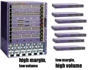
Why would investors agree to sell the company for $50 million? Presumably, they're just accepting reality. Software support businesses rarely attract venture capital, but Linux was a major buzzword for investors earlier in the decade. The trouble with support as a business model is that expenses grow linearly with revenue: as you add customers, you have to grow headcount to handle them. Expenses for a product company grow at a far slower rate, one can increase sales by 2x while increasing expenses by less than 2x.

So far as I can tell adoption of Linux in the embedded space is still growing robustly, displacing commercial RTOSes. The economic benefit of avoiding a per-unit software royalty is compelling. The expertise to bring up Linux on a new board is quite common now, companies can beef up their own teams rather than pay for support from MontaVista or Wind River.


Update: In the comments teich points out Business Review Online shows a somewhat different funding schedule:

MontaVista   9.0   Series A
MontaVista  23.0   Series B
MontaVista  28.0   Series C
MontaVista  12.0   Series D
MontaVista   3.0   individual investment
MontaVista  21.0   Series E

After the $21 million round, MontaVista appears to have taken in another $3.7 million. Altogether this matches the $100 million quotes elsewhere, though I've no idea why some of these funding events are not in Edgar.

Monday, September 28, 2009

49.710269618056 Days

Western Digital recently corrected a firmware issue in certain models of VelociRaptor where the drive would erroneously report an error to the host after 49 days of operation. Somewhat inconveniently for RAID arrays, if all drives powered on at the same time they would all report an error at the same time.

Informed speculation: the drive reports an error after exactly 49 days, 17 hours, 2 minutes, 47 seconds, and 294.999 milliseconds of operation. That is the moment where a millisecond timer overflows an unsigned 32 bit integer.

WD VelociRaptor

Thursday, September 17, 2009

Jasper Forest x86

Intel has a long but uneven history in the embedded market. In the early days of the personal computer Intel released the 80286 as a followon to the original 8086. There actually was an 80186: it was a more integrated version of the 8086 aimed at embedded applications. Intel's interest in embedded markets has waxed and waned over the years, but it is an area where Intel still has room for significant growth.

I wrote about x86 for embedded use about a year and a half ago, with four main points:

  • Volume Discounts
    PC pricing thresholds at 50,000 units have to be rethought for a less homogenous market
  • System on Chip (SoC)
    Board space is at a premium, we need fewer components in the system
  • Production lifetime
    These systems are not redesigned every few months, chips have to remain in production longer
  • Power and heat
    Airflow is more constrained, and the system has other heat generating components besides the CPU complex
Nehalem vs Jasper Forest

At the Intel Developer Forum next week Intel is expected to focus on embedded applications for its products. In advance of IDF Intel announced the Jasper Forest CPU, a System on Chip version of Nehalem. It is based on a 1, 2, or 4 core CPU plus an integrated PCI-e controller, so it does not need a separate northbridge chip. Intel also committed to a 7 year production lifetime, allowing the part to be designed into products which will remain on the market for a while. I'd speculate that Intel will offer industrial temperature grade parts as well, perhaps at lower frequencies.

Jasper Forest is particularly suited for and aimed at storage applications. It has additional hardware for RAID support (presumably XOR & ECC generation), and a feature to use main memory as a nonvolatile buffer cache. When loss of power is detected the chip will flush any pending writes out to RAM and then set the DRAM to self-refresh before shutting down. By including a battery sufficient to power the DRAM, the system can avoid the need for a separate nonvolatile data buffer like SRAM.

This is a good approach for Intel: target silicon at specific high margin, growing application areas. Go for markets with moderate power consumption requirements, as x86 is clearly not ready for small battery powered applications like phones. Ars Technica discusses Intel's upcoming weapon for getting into mobile and other battery powered markets, a version of their 32nm process which reduces leakage current to almost nothing. An idle x86 would consume essentially no power, which would be huge.

Wednesday, July 29, 2009

Embedded Linux Market Share

Last week Wind River, now a subsidiary of Intel, announced that it had taken the lead in the share of embedded Linux revenue.

ALAMEDA, CA - July 22, 2009 - Wind River, a wholly owned subsidiary of Intel Corporation, today announced it has been named the embedded Linux market leader by VDC Research Group. Released today in VDC's 2009 Linux in the Embedded Systems Market report, Wind River achieved the market share lead in 2008 with greater than 30 percent of total market revenue, more than seven percentage points over the next closest competitor. Wind River entered the Linux business in 2004 to complement its market-leading, proprietary operating system, VxWorks.

The unnamed "next closest competitor" is MontaVista Software, but the real competition is not between the different embedded software vendors. The real competition is between any commercial Linux vendor versus rolling your own distribution from source. The various kernel distributions for PowerPC and MIPS are easy to download and cross-compile. Assembling a filesystem is not difficult, as discussed in an earlier article on this site. Add busybox and either glibc or uClibc, and you are most of the way to a bootable system.

There are a few areas where embedded Linux vendors provide value, and why I generally advocate purchasing support from them for a Linux development project:

  • The compiler toolchain: Maintaining a cross-compiling toolchain is quite a bit of work. Most importantly, one has to stay on top of CPU bugs. All CPUs ship with bugs, even x86, but a dirty little secret of the RISC SoC business is that they can go to market with more significant problems than Intel or AMD could get away with. So long as the issue can be worked around in the compiler or assembler - by not emitting the problematic sequence of instructions - the chip will ship anyway and rectify problems in later spins. The bugs will be documented in the Errata, but the descriptions are made to sound quite innocuous. CPU developers make sure that the major commercial embedded Linux vendors have the needed workarounds in their toolchain.
  • The kernel development tax: if you look at the version control logs for Linux/MIPS or Linux/PowerPC, the people doing the heavy lifting are often employed at one of the Linux vendors. Those companies have an economic reason to pay for that development. Unfortunately this leads to a variation of the Prisoner's Dilemma: somebody has to fund it. One can either pay for a support contract in order to fund Linux development, or not pay but hope that enough other people do.
  • Proprietary tools: The package management tools and customized Eclipse IDE supplied by these vendors are generally not useful to me, but some of their supplementary tools for profiling or shared library size reduction are quite interesting.

It is sometimes galling to be paying for support for embedded Linux, particularly because the technical support for specific problems has never actually resolved anything for me. Nonetheless I do advocate having at least a minimal contract, using the supplied compiler toolchain and investigating the other tools they provide. It is worth spending some resources for.

(Original press release via Linux For Devices)

Thursday, July 16, 2009

Courgette binary patch compression

Recently on the Chromium blog Google announced an improved binary compression algorithm called Courgette. In the example cited Courgette produced a patch that was only 11% of the size of that produced by bsdiff. The design overview has more details on its operation:

Courgette uses a primitive disassembler to find the internal pointers. The disassembler splits the program into three parts: a list of the internal pointer's target addresses, all the other bytes, and an 'instruction' sequence that determines how the plain bytes and the pointers need to be interleaved and adjusted to get back the original input. We call this an 'assembly language' because we can run an 'assembler' to process the instructions and emit a sequence of bytes to recover the original file.

The non-pointer part is about 80% of the size of the original program, and because it does not have any pointers mixed in, it tends to be well behaved, having a diff size that is in line with the changes in the source code. Simply converting the program into the assembly language form makes the diff produced by bsdiff about 30% smaller.

I haven't checked, but I suspect its disassembler supports x86 only. Chromium runs on Windows, MacOS X, and Linux, which all run primarily on x86 systems.

Courgette is of course aimed at updates to Google's Chrome browser, which is installed in very large numbers and frequently updated. Reducing the size of the updates results in a better user experience. Nifty.


Incremental Patching and Embedded Systems

When first posted, this article launched directly from Courgette into a discussion of incremental patching in embedded systems. In the comments Wayne Scott pointed out that this really wasn't fair: Courgette is purely a way to make binary patches smaller. In fact because Courgette requires the complete original binary in order to generate its diffs, it cannot be used to generate independent incremental patches at all. After clarifying my thinking, I've updated the post and added a bit of segue text.

Let us now turn to the more general subject of patching of embedded systems. Whenever there is a problem in the field, there is a strong temptation to push out a fix as rapidly as possible. Whether called a point patch or a hotfix, the basic idea is to patch just the portion of the software causing issues for that customer. Larger, periodic maintenance releases collect all existing hotfixes (plus additional ongoing maintenance work) into a single release suitable for all deployments. For embedded systems, on general principles I don't favor the use of hotfixes. Though it reduces the bandwidth required for updates, I feel the disadvantages outweigh the advantages:

  1. perhaps obviously, you need management software to apply, remove, and list installed patches
  2. tech support has a larger number of variations to deal with
  3. test load increases rather dramatically. If you have 5 independent patches you may need to test the combinations, up to 2^5=32 variations to test, not just 5.
  4. Frequent updates are not a good thing for most embedded systems. Customers want the gear to fade into the background and just work, making them update and reboot too often becomes a distinct negative.
  5. As described in an earlier article I favor storing the boot images in a raw flash partition, not any sort of filesystem, which would make installation of an incremental patch more complex.

I recommend not trying to maintain the most recent maintenance release plus an ever-growing collection of hotfixes. I suggest instead to revise the maintenance release whenever there is a cutomer problem. If other customers are not experiencing the problem then they need not deploy the new release right away. The main benefit is to avoid having 2^N possible combinations of patches in the field, instead having only N minor maintenance releases. Revving the maintenance release also tends to be treated with more care than a simple hotfix is; rushing the process is rarely beneficial.

Friday, November 28, 2008

The Six Million Dollar LibC

Android Today, Gentle Reader, we will examine the Bionic library, a slim libc developed by Google for use in the Android mobile software platform. Bionic is clearly tailored for supporting the Android system, but it is interesting to see what might be done with it in other embedded system contexts.

Google's stated goals for Bionic include:

  1. BSD license: Android uses a Linux kernel, but they wanted to keep the GPL and LGPL out of user space.
  2. Small size: glibc is very large, and though uClibC is considerably smaller it is encumbered by the LGPL.
  3. Speed: designed for CPUs at relatively low clock frequencies, Bionic needs to be fast. In practice this seems to drive the decisions of what to leave out, rather than any special Google pixie dust to make code go fast.

In this article we'll delve into the Bionic libc via source inspection, retrieved from the git repository in October 2008. The library is written to support ARM CPUs, though some x86 support is also present. There is no support for other CPU architectures, which makes it a bit inconvenient as all of my current systems are PowerPC or MIPS. Nonetheless I'll concede that for the mobile phone market which Bionic targets, ARM is the only architecture which matters.

As one might expect for a BSD-licensed libc, a significant amount of code is sourced from OpenBSD, NetBSD, and FreeBSD. Additional BSD-licensed bits come from Sun and public domain code like the time zone package. There is also a significant amount of new code written by Google, particularly in the pthread implementation.


C++ support

So what is different about the Bionic libc versus glibc? The most striking differences are in the C++ support, as detailed in the CAVEATS file:

  • The Bionic libc routines do not handle C++ exceptions. They neither throw exceptions themselves, nor will they pass exceptions from a called function back through to their caller. So for example, if the cmp() routine passed to qsort() throws an exception the caller of qsort() will not see it.
     
    Support for C++ exceptions adds significant overhead to function calls, even just to pass thrown exceptions back to the caller. As Android's primary programming language is Java, which handles exceptions entirely within the runtime package, the designers chose to omit the lower level exception support. C++ code can still use exceptions internally, so long as they do not cross a libc routine. In practice, it would be difficult to actually guarantee that exceptions never try to transit a library routine.

  • There is no C++ Standard Template Library included. Developers are free supply their own, such as the free SGI implementation.

Lack of exceptions is obviously a big deal for C++ programmers, but nonetheless we'll push on.


libpthread

The pthread implementation appears to be completely new and developed by Google specifically for Android. It is, quite deliberately, not a complete implementation of POSIX pthreads. It implements those features necessary to support threads in the Dalvik JVM, and only selectively thereafter.

In other embedded Linux environments, the pthread library is crucial. There are a large number of developers in this space from a vxWorks background, to whom threads are simply the way software should be written. So we'll spend a bit more time delving into libpthread.

  • Mutexes, rwlocks, condvars, etc are all implemented using kernel futexes, which makes the user space implementation impressively simple. It seems a little too simple actually, I intend to spend a bit more time studying the implementation and Ulrich Drepper's futex whitepaper.

  • There is no pthread_cancel(). Threads can exit, but can not be killed by another thread.

  • There is no pthread_atfork(). This routine is useful if you're going to fork from a threaded process, allowing cleanups of resources which should not be held in the child. I've mostly seen pthread_atfork() used to deal with mutex locking issues, and need to study how the use of futexes affects fork().

  • Thread local storage is implemented, with up to 64 keys handled. Android reserves several of these for its own use: the per-thread id and errno, as well as two variables related to OpenGL whose function I do not understand. Interestingly the ARM implementation places the TLS map at the magic address 0xffff0ff0 in all processes. This technique is presumably part of the Google performance enhancing pixie dust.

  • POSIX realtime thread extensions like pthread_attr_{set,get}inheritsched and pthread_attr_{set,get}scope are not implemented. Frankly I've never worked on a system which did implement these APIs and am completely unfamiliar with them, so I don't find their omission surprising.

I haven't drawn a final conclusion of the Bionic pthread implementation yet. It is pleasingly simple, but lack of pthread_atfork() is troublesome and use of a magic address for the TLS map may make porting to other architectures more difficult. I need to get this puppy running on a PowerPC system and see how well it works.


Miscellaneous notes

In the course of digging through the library I generated a number of other notes, which don't really clump into categories. So I'm simply going to dump it all upon the Gentle Reader, in hopes that some of it is useful.

  • The README says there is no libm, though the source for libm is present with a large number of math routines. I need to investigate further whether it really works, or whether the README is out of date.

  • There is no wchar_t and no LOCALE support. I think this is fine: wchar_t is an idea whose time has come... and gone. The world has moved on to Unicode with its various fixed and variable width encodings, which the wide character type is not particularly useful for.
    I've used ICU in recent projects for internationalization support, and this is also what Google suggests in the README for Bionic.

  • There is a shared memory region of configuration properties. For example, DNS settings are stored in shared memory and not /etc/resolv.conf. The Android API also makes this shared memory configuration store available to applications via property_get() and property_set().

  • As one might expect, the stdio/stdlib/string/unistd implementation comes from OpenBSD, NetBSD, and FreeBSD with minimal changes. The only change I noticed was to remove the LOCALE support from strtod() (i.e., is the decimal point a period or a comma? In the Bionic library it is always a period).

  • There is no openlog() or syslog() implementation. There is a __libc_android_log_print() routine, to support Android's own logging mechanism.

  • Bionic uses Doug Lea's malloc, dlmalloc. Bionic also provides a hash table to track allocations looking for leaks, in malloc_leak.c.

  • There is no pty support that I can find, and no openpty(). There are reports of people starting an SSH daemon on a jailbroken Android device, so presumably there is some pseudo-terminal implementation which I've missed.

  • There are no asynchronous AIO routines like aio_read() or aio_write().

  • Bionic contains an MD5 and SHA1 implementation, but no crypt(). Android uses OpenSSL for any cryptographic needs.

  • Android dispenses with most file-based Unix administration. Bionic does not implement getfsent, because there is no /etc/fstab. Somewhat incongruously there is a /var/run/utmp, and so getutent() is implemented.

  • Android implements its own account management, and does not use /etc/passwd. There is no getpwent(), and getpwnam()/getpwuid() are implemented as wrappers around an Android ID service. At present, the Android ID service consists of 25 hard-coded accounts in <android_filesystem_config.h>

  • Bionic isn't finished. getprotobyname(), for example, will simply print "FIX ME! implement getprotobyname() __FILE__:__LINE__"

  • There is no termios support (good riddance).

 
Conclusion

Bionic is certainly interesting, and pleasingly small. It also represents a philosophical outlook of keeping the GPL some distance away from the application code.

Bionic is a BSD-based libc with support for Linux system calls and interfaces. If the lack of C++ exceptions or other limitations prove untenable, the syscall and pthread mutex implementation could be repurposed into the heavier FreeBSD/NetBSD/OpenBSD libc, though handling thread cancellation using the Bionic mutexes could require additional work.


Postscript

If you don't understand the reference in the title of this article, don't fret: you have simply not watched enough bad 1970's American television.

Update: In the comments, Ahmed Darwish points out another Android-related article discussing the kernel and power management interfaces Google added.

Update2: Embedded Alley is working on a MIPS port of the Android software.

Update3: In the comments Shuhrat Dehkanov points out an interview with David Turner, who works at Google on the Bionic implementation. Shuhrat also notes that you might have to log in to Google Groups to see the attachment. "Here is an overview by David Turner (though non-official) which answers some of the questions/unclear parts in your article."

Wednesday, July 23, 2008

The Control Plane is not an Aircraft

In my industry at least, the high end of the margin curve is dominated by modular systems: a chassis into which cards can be added to add features, increase capacity, etc. Products at the cheaper end of the spectrum tend to be a fixed configuration, a closed box which does stuff but is not terribly expandable (often called a pizza box). The fixed configuration products sell in much larger volumes, but margins are lower.

Chassis has high margins and low volume, fixed config has lower margins and high volumes
Block diagram of fixed configuration system, showing CPU attached to ASICs via a PCI bus

In a pizza box system the control plane between the CPU and the chips it controls tends to be straightforward, as there is sufficient board space to route parallel busses everywhere. PCI is often used as the control interface, as most embedded CPUs contain a PCI controller and a lot of merchant silicon uses this interface.

In a chassis product, there is typically a central supervisor card (or perhaps two, for redundancy) controlling a series of line cards. There are a huge number of options for how to handle the control plane over the backplane, but they mainly fall into two categories: memory mapped and message oriented. In todays article we'll examine the big picture of control plane software for a modular chassis, and then dive into some of the details.


Memory Mapped Control Plane

A memory-mapped chassis control plane extends a bus like PCI over traces on the backplane.

Memory mapped chassis system with PCI over the backplane

To the software, all boards in the chassis appear as one enormous set of ASICs to manage.


Message Passing Control Plane

Alternately, the chassis may rely on a network running between the supervisor and line cards to handle control duties. There are PHY chips to run ethernet via PCB traces, and inexpensive switch products like the Roboswitch to fan out from the supervisor CPU out to each slot in the chassis.

Message Passing chassis system with ethernet links

This system requires more software, as each line card runs its own image in addition to the supervisor card. The line cards receive messages from the supervisor and control their local ASICs, while the supervisor has to handle any local ASICs directly and generate messages to control the remote cards.


Programming Model

As the Gentle Reader undoubtedly already knows, the programming model for these two different system arrangements will be radically different.

Memory mapped
ASICs are mapped in as pointers
Message Passing
ASICs controlled using, erm, messages. Yeah.
volatile myHWRegisters_t *p;

p = <map in the hardware>
p->reset = 1;
myHWMessage_t msg;

msg.code = DO_RESET_ASIC;
send(socket, &msg, sizeof(msg), 0);
Perhaps that was obvious. Moving on... At first glance the memory mapped model looks pretty compelling:
  • it the same as a fixed configuration product, allowing easy code reuse
  • in the message passing model you still have to write memory map code to run out on the line card CPUs, and then you have to write the messaging layer

 
Hot Swap Complicates Things

A big issue in the software support for a chassis is support for hot swap. Cards can be inserted or removed from the chassis at any time, while the system runs. The software needs to handle having cards come and go.

With a message passing system hotswap is fairly straightforward to handle: the software will be notified of insertion or removal events, and starts sending messages. If there is a race condition where a message is sent to a card which has just been removed, nothing terrible happens. The software needs to handle timeouts and gracefully recover from an unresponsive card, but this isn't too difficult to manage.

With a memory mapped chassis, hot insertion is relatively simple. The software is notified of an insertion event, and maps in the hardware registers. Removal is not so simple. If the software is given sufficient notice that the card is being removed, it can be cleanly unmapped and safely removed. If the card is yanked out of the chassis before the software is ready, havoc can ensue. Pointers will suddenly reference a non-existant device.


Blame the Hardware

So card removal is difficult to handle robustly in a chassis which memory-maps the line cards.

CompactPCI card showing microswitch and hot-swap LED

Ideally the hardware should help the software handle card removal. For example CompactPCI cards include a microswitch on the ejector lever, which signals the software of an imminent removal. The user is supposed to flip the switch and wait for an LED to light up, an indication that the card is ready to be removed. Of course, people ignore the LED and pull the card out anyway if it takes longer than 1.26 seconds... we did studies, and stuff... ok I just made that number up. Card removal is often then made into a software problem: "Just add a CLI command to deprovision the card, or something."

This makes for a reasonably nasty programming environment: to be robust you have to constantly double-check that the card is still present. Get a link up indication from one of the ports? Better check the card presence before trying to use that port, in case the linkup turns out to be the buswatcher's 0xdeadbeef pattern. Read an indication from one of the line cards that its waaaaay over temperature? Check that it is still there before you begin shutting the system down, it might just be a garbage reading.


Pragmatism is a Virtue

There is a maxim in the marketing strategy for a chassis product line: never let the customer remove the chassis from the rack - they might replace it with a competitors chassis. You can evolve the design of the line cards and other modules, but they must function in the chassis already present at the customer site. Backplane designs thus remain in production for a long time, often lasting through several generations of card designs before finally being retired. Though the Gentle Reader might have a firm preference for one control plane architecture or another, the harsh reality is that one likely has to accept whatever was designed in years ago.

So we'll spend a little time talking about the software support for the two alternatives.


Thoughts on Memory Mapped Designs

Software to control a hardware device does not automatically have to run in the kernel. There are only a few things which the kernel absolutely has to do: Driver code can run in user space

  1. map the physical address of the device in at a virtual address
  2. handle interrupts and mask the hardware IRQ
  3. deal with DMA, as this involves physical addressing of buffers

Everything else, all of the code to initialize the devices and all of the higher level handling in response to an interrupt, can go into a user space process where it will be easier to debug and maintain. The kernel driver needs to support an mmap() entry point, allowing the process to map in the hardware registers. Once mapped, the user process can program the hardware without ever calling into the kernel again.


Thoughts on Message Passing Designs

First, an assertion: RPC is a terrible way to implement a control plane. One of the advantages of having CPUs on each card is the ability to run operations in parallel, but using remote procedure calls means the CPUs will spend a lot of their time blocked. The control plane should be structured as a FIFO of operations in flight, without having to wait for each operation to complete. If information is needed from the remote card it should be structured as a callback, not a blocking operation.

It is tempting to implement the control communications as a series of commands sent from the supervisor CPU to the line cards. Individual commands would most likely be a high level operation, requiring the line card CPU to implement a series of accesses to the hardware. The amount of CPU time it takes for the supervisor to send the command would be relatively small compared to the amount of time the line card will spend implementing the command, likely accentuated by a significantly faster CPU in the supervisor. Therefore the supervisor will be able to generate operations far faster than the line cards can handle them. In networking gear this is most visible when a link is flapping [an ethernet link being established and lost very rapidly] where commands are sent each time to reconfigure the other links. If the flapping persists, you either cause a failure by overflowing buffers in the control plane or start making the supervisor block while waiting for the line card to drain its queue. Either way, its bad.

One technique to avoid these overloads is to have the supervisor delay sending a message for a short time. If additional operations need to be done, the supervisor can discard the earlier updates and send only the most recent ones. The downside of delaying messages in this way is that it is a delay, and responsiveness suffers.

Another technique involves a somewhat more radical restructuring. The line card most likely contains various distinct bits of functionality which are mostly decoupled. Falling back to my usual example of networking gear, the configuration of each port is mostly independent of the other ports. Rather than send a message describing the changes to be made to the port, have the supervisor send a message containing the complete port state. Because each message contains a complete snapshot of the desired state of the port, the line card can freely discard older messages so long as it implements the one most recently sent.

Control Plane State Coalescing

By structuring the control messages to contain a desired state, you allow the remote card to degrade gracefully under load. Under light load it can probably handle every message the supervisor sends, while under heavier load it will be able to skip multiple updates to the same state.

Note that the ordering of updates is lost, as events can be coalesced into a different order than that in which they were sent. This coalescing scheme can only work if the various bits of state really are independent, if one state depends on an earlier update to a different state then they are not independent.


Closing Thoughts

Gack, enough about control plane implementation already.

The comments section recently converted over to Disqus, which allows threading so the Gentle Reader can reply to an earlier comment. Anonymous comments are enabled for now, though if comment spam becomes a problem that may change.